The market demand for industrial applications is increasing day by day, and data acquisition system is the key equipment. They are usually used to detect temperature, flow, liquid level, pressure and other physical quantities, and then convert the analog signals corresponding to these physical quantities into high-resolution digital information, which is then further processed by software. Such systems are increasingly demanding for accuracy and speed. These data acquisition systems consist of amplifier circuits and analog-to-digital converters (ADC), whose performance has a decisive impact on the system.
However, the overall accuracy is also affected by the ADC's input driver, which is used to buffer and amplify the input signal. In addition, a bias signal must be added or a fully differential signal must be generated to cover the ADC's input voltage range and meet its common-mode voltage requirements, without altering the original signal in the process. Programmable gain instrumentation amplifiers (PGIA) are commonly used as input drivers. In this paper, we propose a combination of input driver and ADC, through which very precise conversion results can be achieved to build a high quality data acquisition system.
For example, the LTC6373 is a PGIA suitable for high precision data acquisition systems. In addition to a fully differential output, it has high DC accuracy, low noise, low distortion (see Figure 2), and a high bandwidth of 4 MHz with gains of 1/4 to 16. The ADC can be driven directly through it and is therefore suitable for many signal conditioning applications.
The circuit in Figure 1 shows an example of using the LTC6373 to drive a precision AD4001 / AD4020 with a 20-bit resolution of 1.8 MSPS.
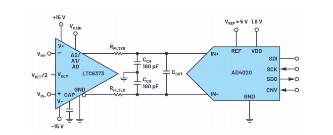
Figure 1. Example of a circuit that drives a precision ADC
In this circuit, the LTC6373 is DC coupled at the input and output, thus eliminating the need for a transformer to drive the ADC. The gain can be set between 0.25 V/V and 16 V/V via pins A2/A1/A0. In Figure 1, the LTC6373 uses a differential input-to-differential output configuration and a ±15 V symmetric supply voltage. Alternatively, the input can be a single-ended input while the output remains a differential output.
In Figure 1, the output common-mode voltage is set to VREF/2 via the VOCM pin. This enables the output level conversion of LTC6373. Each output of the LTC6373 varies between 0 V and VREF, so there is a differential signal at the ADC input of 2 x VREF amplitude. The RC network between the LTC6373 output and the ADC input forms a single-pole low-pass filter that reduces the current burr generated when switching capacitors at the ADC input. At the same time, the low-pass filter limits the broadband noise.
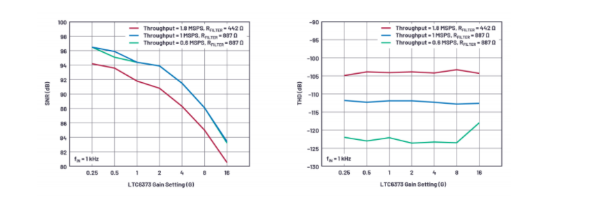
Figure 2. 4001 / AD4020 (left) and THD (right) performance driven by the LTC6373
Figure 2 shows LTC6373 signal-to-noise ratio (SNR) and total harmonic distortion (THD), in the entire input voltage range (10 v p - p) drive AD4020 SAR ADC (high impedance state model). Satisfactory results can be obtained when the throughput is 1.8 MSPS and the RFILTER is 442 Ω. At 1 MSPS or 0.6 MSPS, the manufacturer recommends an RFILTER of 887 Ω.
The LTC6373 drives most SAR ADCs with differential inputs without the need for additional ADC drivers. However, in some applications, a separate ADC driver can be used between the LTC6373 and the precision ADC to further improve the linearity of the signal chain.
| 零件編號 | 描述 | |
|---|---|---|
| LTC6228IS6#TRMPBF Linear Technology |
線性 - 放大器 - 儀表、運算放大器、緩衝放大器, IC OPAMP GP 1 CIRCUIT TSOT23-6 | RFQ |
| LTC6228HS8#PBF Linear Technology |
線性 - 放大器 - 儀表、運算放大器、緩衝放大器, IC OPAMP GP 1 CIRCUIT 8SO | RFQ |
| LTC6228HS6#TRMPBF Linear Technology |
線性 - 放大器 - 儀表、運算放大器、緩衝放大器, IC OPAMP GP 1 CIRCUIT TSOT23-6 | RFQ |
| LTC6228HDC#TRMPBF Linear Technology |
線性 - 放大器 - 儀表、運算放大器、緩衝放大器, IC OPAMP GP 1 CIRCUIT 6DFN | RFQ |
| LTC2050HVMPS6#TRMPBF Linear Technology |
線性 - 放大器 - 儀表、運算放大器、緩衝放大器, IC OPAMP ZER-DRIFT 1CIR TSOT23-6 | RFQ |
Traction inverters are the main battery drain components in electric vehicles (EVs), with power levels up to 150kW or higher. The efficiency and performance of traction inverter directly affect the driving range of electric vehicle after a single charge. Therefore, in order to build the next generation of traction inverter systems, silicon carbide (SiC) field effect transistor (FET) is widely used in the industry to achieve higher reliability, efficiency and power density.
Do you know the 8 application circuits of operational amplifiers?
This technical presentation requires an understanding of how to configure an operational amplifier in a typical gain control circuit. The applications of linear and nonlinear digital potentiometers are discussed. This article gives an overview of the basic techniques required to convert audio and other potentiometer/op amp applications from conventional mechanical potentiometers to solid state potentiometers
The current in an electronic circuit usually has to be limited. In USB ports, for example, excessive current must be prevented to provide reliable protection for the circuit. Also in the power bank, the battery must be prevented from discharging. Too high discharge current results in too large voltage drop of the battery and insufficient supply voltage of downstream devices
Using advanced real-time control technologies such as motor control circuits with higher power density, higher integration and more efficient systems, better acoustic performance of the system can be achieved
Brushless direct current (BLDC) motors have been widely used in household appliances, industrial equipment and automobiles. While brushless DC motors offer a more reliable and maintainable alternative to traditional brushless motors, they require more sophisticated electronics to drive them
How to achieve precise motion control in industrial actuators
The NCP51820 is a 650 V, high-speed, half-bridge driver capable of driving gallium nitride (" GaN ") power switches at dV/dt rates up to 200 V/ns. The full performance advantages of high voltage, high frequency and fast dV/dt edge rate switches can only be realized if the printed circuit board (PCB) can be properly designed to support this power switch. This paper will briefly introduce NCP51820 and the key points of PCB design of high performance GaN half bridge grid driver circuit using NCP51820