GTLP6C817 is a low driver clock driver that provides TTL to GTLP signal level conversion (and vice versa). The device provides a high-speed interface between the interface card working in the TTL logic layer and the backplane working in the GTLP logic layer. High-speed backplane operation is GTLP reduces output wobble (< 1V), reducing the input threshold level and output edge rate control as a direct result.
Logic diagram
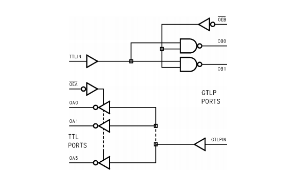
Edge rate control minimizes bus setup time. GTLP is a derivative of Fairchild Semiconductor's Shooting Transceiver Logic (GTL) JEDEC standard JESD8-3. Fairchild's GTLPS have internal edge rate control and are process, voltage, and temperature (PVT) compensated. Its function is similar to BTL and GTL, but the output level and receiving threshold are different. The GTLP output LOW level is usually less than 0.5V, the output HIGH level is 1.5V, and the receiver threshold is 1.0V