As new markets and applications continue to emerge, the demand for mobile data has skyrocketed. There is no solution other than deploying more cellular sites at greater density. These factors will directly affect the design of macro base station, small base station and femtobase station products. Now that radios support multi-band operation, power amplifier (PA) design engineers are trying to push the output power of PA to higher limits/levels.

This article focuses on the case where 80 W PA is included in multiple PA systems. 1400 W Long Range Radio Unit (RRU) platforms are becoming more common. However, network operators hope that these RRU will increase coverage density while being more energy efficient, reliable, and compact. The point of load (PoL) needs to operate over a wide input voltage and wide operating temperature range and, more importantly, must be cost-effective.
However, for applications requiring 500 W or more power, it is difficult to design the magnetic components of the secondary circuit and conduct loss management in active clamp forward converter designs due to the need for advanced control schemes to maintain the delay timing between the active clamp and the main switch gate drive. This article describes a scalable and stackable -48 VDC PoL solution that addresses the high density power consumption of these high density networks due to the surge in network traffic.
Abstract
Telecommunications and wireless network systems typically operate on a -48 VDC power supply. Because DC power is simpler, a backup power system can be built using batteries without the need for an inverter. Direct current can be stored in batteries; When the mains is interrupted, these batteries can be used to provide continuous power for a period of time. However, -48VDC must first be efficiently converted to positive intermediate bus voltage and then boosted to power the PA, or stepped down to positive working power for use by digital baseband units (BBUS). Power supplies with capacities of 100 W to 350 W are sufficient to cover many application needs.
Forward converters are a good choice and have been widely used in telecom Bbus and RRU for many years. As the demand for mobile data continues to grow, new markets and applications continue to emerge. Forward converters now face serious challenges, especially with the output power requirements of these new radio designs exceeding 500 W. This paper proposes a stackable and interleaved multiphase high voltage reverse buck-boost controller that addresses all of these needs/challenges to meet the requirements of today's 5G telecom equipment. But first, where did -48VDC come from? Why do you need a negative potential?
Typical telecommunication DC power supply system
Telecommunications and wireless networks typically run on -48VDC power, but why? In simple terms, the reason for choosing -48 VDC (also known as the positive grounding system) is that it provides enough power to support telecommunications signals and is safer for the human body when conducting telecommunications activities. According to current safety regulations and electrical codes, any circuit operating at or below 50 VDC is a safe low-voltage circuit. Another reason is that -48VDC makes it easy for telecom operators to use 12-V lead-acid batteries in series as backup power to continue supplying power when the grid system fails. -48VDC is still the standard for communications facilities that provide wired and wireless services because it is believed to cause less corrosion to metals (or at least inhibit galvanic corrosion) than positive voltage.
Figure 1 is a diagram of a typical telecommunication DC power supply system, highlighting how -48VDCis created and distributed. The telecommunication DC power supply system usually includes: the national grid system, diesel generators, autonomous AC automatic switching switches (ATS), distribution systems, solar panels or circuit boards, controllers and chargers, rectifiers, backup batteries arranged in series, and corresponding cables and circuit breakers.
Figure 1. Schematic diagram of a typical telecommunication DC power supply system
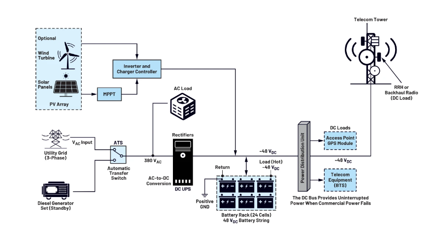
When the power grid is cut off, the diesel generator automatically starts to provide AC power to the DC port system. ATS Synchronizes different power supply voltages to the device. Since most telecommunications equipment in the field requires DC power, alternating current from the grid or a diesel generator is converted to -48VDC by a rectifier. These redundant rectifiers are used to convert AC power to -48VDC power to trickle charge the battery and support critical loads. The battery is in a floating state, and if the rectifier cannot provide -48VDC power, the battery will provide that power for telecommunications equipment or other loads. The BTS or RRH won't notice the difference in the actual power supply, and everything stays up and running. When the power is restored, the rectifier takes over again. In essence, the entire power plant is like a large uninterruptible power supply (UPS).
Limitations of forward converters
Now that we know where -48VDC comes from, let's discuss one of the PoL topologies commonly used in the industry to convert -48VDC to positive voltage. Many telecom PoL designers use active clamp forward converters to achieve reverse-phase buck-boost designs. Other circuit forms are also used, such as push-pull, half-bridge or full-bridge converters. The benefit is that most of the energy leaked by the transformer can be recovered through its near-lossless recovery method. It is important for PoL designers to first understand the basic timing inherent in active clamp reset. In fact, improper sizing of the clamp capacitor can result in increased PoL duty cycle, resulting in transformer saturation and long-term reliability of the main switch. Figure 2 shows a traditional low-side transformer reset active clamp forward converter circuit design. The transformer reset mechanism includes CCLAMP and Q1.
Figure 2. Traditional low-side transformer reset clamp active forward design

Some disadvantages associated with active clamping include the need to accurately determine the size of the clamping capacitance. The larger the capacitance value, the smaller the voltage ripple, but the transient response will be limited. Active clamp forward topology requires the use of advanced control technology to achieve delay timing synchronization between the active clamp and the main switch gate drive. Another disadvantage associated with active clamping is that if clamping to a certain maximum is not achieved, the increased duty cycle may cause the transformer to saturate or place additional voltage stress on the main switch, which can have catastrophic consequences.
Finally, active clamp forward converters are single-stage DC-DC converters. As power levels increase (800 W devices are becoming the norm in 5G systems, for example), multiphase designs will bring even more advantages to these power-intensive applications. Single-phase converters do not provide any of the benefits of using multiphase interleaving. In addition, the active clamp forward design cannot extend similar results from lower output power designs to higher output power. The next section describes the inverting step-boost converter MAX15258. Figure 3 is a typical simplified block diagram of the RRU board power supply for 5G macro base station or femto base station. Hot-swappable controllers are almost universally placed in front of -48 VDC converters. Examples of full-featured -48 VDC hot-swappable power managers include the ADM1073 and LTC4284, both of which are ideal for these applications.
Figure 3.5G macro base station power block diagram

Key IC devices
The MAX15258 is a high-voltage polyphase boost controller with an I2C digital interface that supports up to two MOSFET drivers and four external MOSFETs in single-phase or dual-phase boost/inverse-step-boost configurations. The two controllers can be stacked to form a three-phase or four-phase configuration. The device drives each phase with an appropriate amount of phase shift to eliminate ripple as efficiently as possible. When configured as a reverse-phase buck-boost converter, the MAX15258 has an internal high voltage feedback level converter for differential detection of the output voltage. FIG. 4 is a simplified block diagram for implementing the staggered two-phase step-up design.
Figure 4. Simplified block diagram of two-phase interleaved reverse buck - boost

With this IC, unlike forward converter designs, designers do not need to consider possible (15 to 20 percent) phase imbalances in the design calculation step. The controller relies on a fixed-frequency peak current mode architecture to regulate the output, which provides a fast transient response. A detailed block diagram of the control loop is shown in the device data manual. The device monitors the low-side MOSFET current of each phase via RSENSE and uses differential current to detect the signal to ensure correct active phase current balance behavior when stacking two MAX15258 ics in a host-node configuration. The current imbalance will be applied as feedback to the period-by-cycle current detection circuit, which helps to regulate the load current to achieve current parity between the two phases.
In three-phase or four-phase operation, the node device uses differential (CSIO+, CSIO-) signals to transmit its average current to the host controller. It is this accurate current balancing characteristic that makes the MAX15258 very attractive to PoL designers. Figure 5 shows a four-phase interlacing reverse-phase buck-boost -48 VINto +48 VOUT 800 W power supply where the CSIO+ and CSIO- signals connect the two controllers. Note that the SYNC pins of both devices are also connected to ensure clock synchronization for the coordinated phase interleaving scheme.
Figure 5. Four phase interlacing reverse buck - boost -48VIN to +48VOUT 800 W, CSIO+ and CSIO- signals connect to the controller

Similarly, the MAX15258 is essentially a boost converter that operates at a relatively low frequency. This naturally reduces switching loss, which is the most important power loss factor in these converters. The device supports switching frequencies up to 1 MHz. In a polyphase operation, the phases run in parallel and all run at the same frequency (but interleaved). The total equivalent frequency is N × Freq, where N is the number of phases, but the loss is the frequency loss per converter. The interleaved implementation will offset the ripple current of the output capacitor to some extent. The input ripple current is greatly reduced, so smaller input inductors can be used.
The use of ADI's patented coupled inductance (CL) technology also helps to attenuate the output ripple current, making it possible to use less expensive capacitors with lower ripple current ratings. This results in increased efficiency while reducing the overall PoL PCB size. In essence, it provides a large amount of output power at a high equivalent total frequency, but each converter operates at a low frequency in a low loss region. This clever design makes the MAX15258 an advanced solution for -48 VDC conversions.
Active clamp forward topology limits the ability to achieve duty cycles, making it difficult for some VIN and VOUT combinations to work. As telecom Oems combine different frequency bands on the same platform, the ability to support different PA output voltage ranges has become a mandatory requirement. Active clamp forward converters have limited output power. The MAX15258 meets IPC9592B pin gap or PCB conductor spacing requirements and supports peak voltages up to 56 V. The IPC9592B standard provides a formula to calculate the PWB surface clearance at operating voltages from 30 V to ~100 V, i.e. : Clearance (mm) = 0.1 + VPEAK × 0.01 (for example, at 56 V, the gap between the high voltage pin and other pins is 0.66 mm).
Ultimately, active clamp forward converters require too many complex steps to ensure that the transformer does not saturate. However, the MAX15258 automatically inverts the voltage, delivering very high output power with very high efficiency and with excellent (higher) duty cycle capability. These features enable scalable and stackable (up to four-phase) platform designs that provide flexible and stable duty cycle control to accommodate a wide VIN and VOUT range. Figure 6 shows the efficiency curves of the MAX15258 800 W reference design based on coupling inductance under different VINand VOUT conditions. These curves clearly show that the efficiency can reach 98% or more due to the low conduction loss, which is excellent. All of this is achieved at a low relative BOM cost.
Figure6. Efficiency curves of the MAX15258 CL 800W reference design under different VIN and VOUT conditions

Through the I2C digital interface, users can read back a large amount of telemetry information from the MAX15258, including VIN, VOUT, phase current, and fault status.
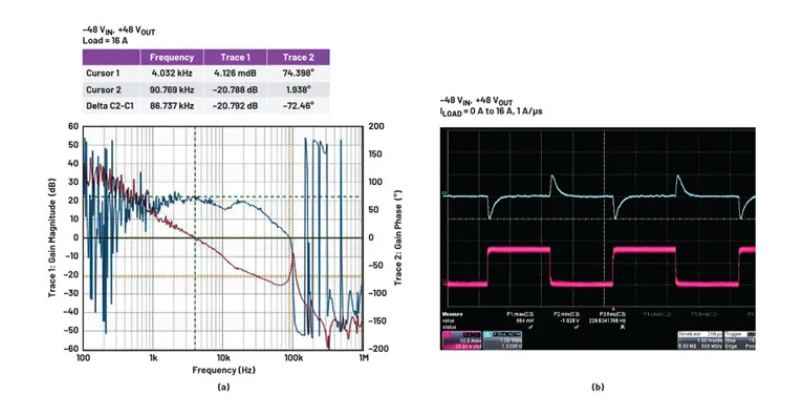
In addition, the output voltage can be set dynamically via a digital interface. Figure 7a shows the Bode diagram of the MAX15258 CL 800 W reference design measured at steady-state load current operating at -48 VIN and +48 VOUT (16 A IOUT). The results show that the phase margin is 74.4° and the gain margin is -20.7 dB. Figure 7b shows the load transient response curve. It can be observed that the switch edge is very clean, the overshoot is almost zero, and the ringing is zero.
Figure 7.(a) Bird plot measured at steady-state load current operation; (b) Load transient response: CH3-VOUT (AC),ILOAD; Ch2 - ILOAD, 10 A/div
Conclusion
Network operators will have to install more small cell towers in more places and faster than ever before. Of course, the PoL in these products needs to be very efficient, with a rated power conversion efficiency of at least 98%. The MAX15258 High voltage reverse buck-boost controller is designed to be cost-effective, efficient and scalable, allowing easy addition and removal of phases on the same PCB layout. These advantages help power converter designers improve power conversion efficiency. Analog Devices will continue to address these and similar challenges, leveraging its extensive expertise in power architecture to develop additional -48 VDC high-power conversion solutions for the 5G market.
Heisener Electronic is a famous international One Stop Purchasing Service Provider of Electronic Components. Based on the concept of Customer-orientation and Innovation, a good process control system, professional management team, advanced inventory management technology, we can provide one-stop electronic component supporting services that Heisener is the preferred partner for all the enterprises and research institutions.