The power electronics world has woken up to the benefits of gallium nitride—big time. Activity in the relevant press, at trade shows and at conferences has been dominated by discussions concerning the increases in efficiency and power that can be achieved by moving from silicon MOSFETs to GaN solutions. Analysts vary in their growth expectations, but nearly all expect at least a 24% CAGR from now until 2027, with some estimates much higher, especially in certain key market segments as diverse as industrial, consumer, telecom and automotive. This much we know. However, today, in addition to the widespread availability of discrete GaN HEMT devices, we are seeing the emergence of integrated GaN solutions from leading GaN manufacturers that build on the intrinsic benefits of GaN and have the potential to deliver even better performance.
First, it is worth saying that the integrated solution is not a panacea. Depending on how the circuit design is partitioned, it may be preferable to use a discrete high-efficiency GaN switch. This is especially the case if a specific driver is required, if the driver is already included within the controller or for higher power levels above, say, 1 kW, as some integrated solutions cannot yet be paralleled. For such applications and others that require maximum design flexibility, manufacturers like Innoscience offer a wide range of discrete parts, ranging from 30 V and up to 700 V with various on-resistances.
But in many other cases, an integrated solution (e.g., driver + GaN HEMTs; half-bridge + driver) can shrink design volume, offer increased power levels and reduce component count (smaller BOM). Let us take as an example the ISG3201, a 100-V product in Innoscience's SolidGaN family that combines two 100-V 2.3-mΩ enhancement-mode GaN devices with a 100-V half-bridge gate driver. Presented in a 30-pin LGA package measuring just 5 x 6.5 x 1.12mm, the device targets high-frequency buck converters, half-bridge or full-bridge converters, Class D audio amplifiers, LLC converters and power modules in applications including motor drivers, AI, servers, telecoms and supercomputers. The below figure shows a simplified schematic of the device.
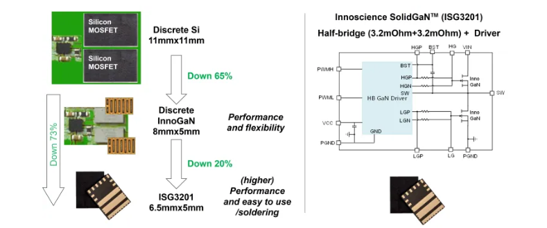
A comparison of the half-bridge circuit implemented using high-spec silicon MOSFETs, discrete GaN devices and the integrated ISG3201 shows that the discrete GaN solution is 66% smaller in area, as we might expect, but that the integrated SolidGaN part is a further 19% smaller, or 73% smaller than the silicon circuit. The above figure also explains how the ISG3201 minimizes the need for external components.
The driving resistor, the bootstrap and the VCC capacitor are all also included in the package, eliminating seven components (four resistors and three capacitors). A further benefit is that because all of these functions are integrated, the gate-loop inductance is reduced, as is the power-loop inductance, typically by 40%. The reduction in parasitics leads to less ringing, for example, and reduced overshoot. This not only increases efficiency and simplifies design but also improves reliability, as overshoot is minimized to 4 V, 80% less than some competitors. Also, fewer clamping components are required.
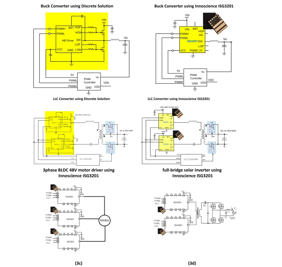
The design also simplifies power stage layout. In some configurations, the switch node is between VIN and PGND, which simplifies device construction but requires extra external components. The Innoscience design in the below figure shows that the switch node is at the edge, so only a simple decupling capacitor is required between VIN and PGND, and the switch node connects to the external circuit. Depending on the power stage topology chosen, this can save many components.

The below figure shows the simplicity of the circuits required for a buck (top), LLC (middle), three-phase BLDC (bottom, left) and full-bridge solar inverter (bottom, right). Using a discrete approach would require more components, as shown in the top figure (buck) and middle figure (LLC).
The integrated design has manufacturing benefits, too. Mounting discretes that come in a fine-pitch wafer-level chip-scale package is difficult to control and also limits the amount of copper that can be used on the PCB. Although GaN typically runs cooler than silicon because it is more efficient, at high power levels, more copper to improve thermal performance is desirable, even essential. By using integrated packages with a larger pin pitch, 2-oz. copper can be used rather than one ounce, which is the practical limit for fine-pitch discretes.
This reduces power loss and increases efficiency, extending the practical useful power range of GaN technology. Tests have shown that the efficiency of half-bridge designs using integrated parts, such as the ISG3201, is 0.3% higher than implementations using discrete GaN devices due to the increase in PCB copper. Is 0.3% higher than implementations using discrete gan devices due to the increase in PCB copper.
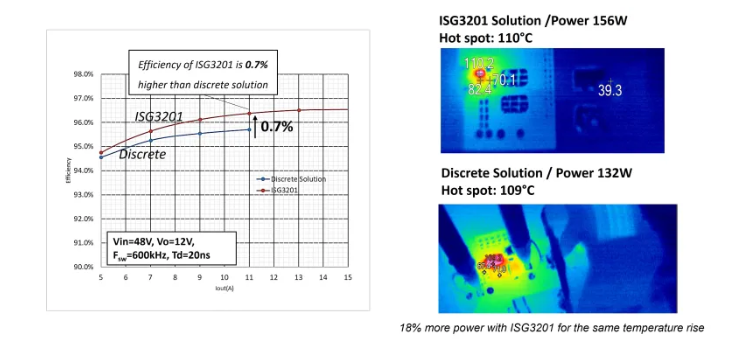
If we consider a 48-/12-V DC/DC converter module running at 1 MHz, we see that these efficiency improvements start to make a significant difference. The below figure shows that an overall improvement in efficiency of 0.7% can be achieved by implementing the design using the example. ISG3201 integrated half-bridge rather than a discrete solution. The thermal plots prove that for the same temperature rise, this increase in efficiency means that 18% more power can be achieved using the integrated approach.
Motor driver application
The below figure presents the example of a 500-W motor driver application (1,000 W peak power), such as what might be used in an e-mobility application. In this design, three compact SolidGaN ISG3201 half-bridge ICs can replace six TO-220 - packaged 90-V/4-mΩ silicon MOSFETs and three half-bridge driver ICs, plus a handful of external components, resulting in space savings of nearly 90%. A reference design and evaluation board are available.
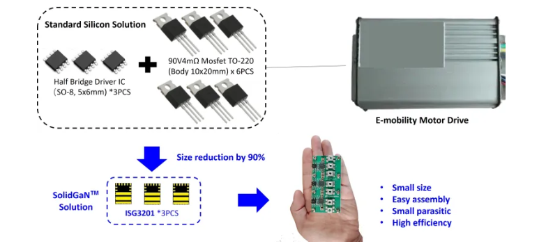
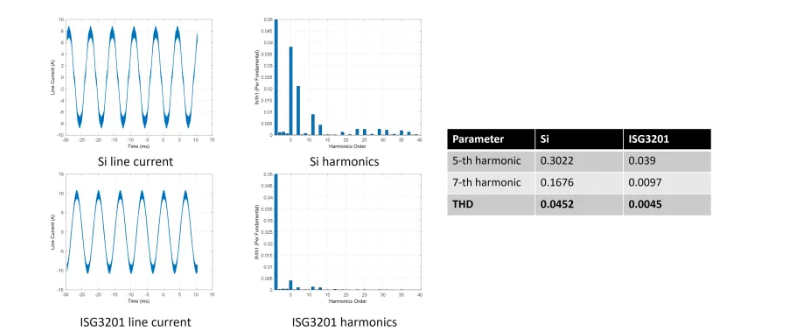
The use of GaN results in lower total harmonic distortion by at least one order of magnitude. This results in less torque ripple, less overcurrent and fewer winding losses. The motor runs smoother with less audible noise, which has positive implications for reliability and motor life.
As we can see, integrated solutions offer many benefits, including size and efficiency, yet discrete GaN solutions still provide the ultimate in design flexibility and may be the only available choice at higher powers until further paralleling of integrated devices is achieved (this is in the roadmap). But whatever your preference, GaN—in some format—is probably the answer.
About US
Heisener Electronic is a famous international One Stop Purchasing Service Provider of Electronic Components. Based on the concept of Customer-orientation and Innovation, a good process control system, professional management team, advanced inventory management technology, we can provide one-stop electronic component supporting services that Heisener is the preferred partner for all the enterprises and research institutions.