Abstract
An ideal diode uses a low-on-resistance power switch (typically a MOSFET) to simulate the unidirectional current behavior of the diode, but without the voltage drop loss of the diode. With additional back-to-back MOSFETs and control circuits, the solution can provide additional system control functions such as priority source selection, current limiting, surge limiting, and more. In traditional solutions, these functions are scattered across different controllers, so achieving complete system protection can be complex and cumbersome. Here we will examine the main circuit specifications of the ideal diode and present an application example and a new ideal diode solution that also integrates in a single IC additional features needed to achieve overall system protection.
Ideal diode basics
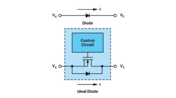
Figure 1 shows a basic ideal diode with an n-channel power MOSFET. Position the MOSFET in the proper orientation so that its eigendiode is in the same functional direction as the diode to be simulated (above). When VA is higher than VC, current can flow naturally from left to right through the intrinsic diode. When the current flows in this direction, the control circuit makes the MOSFET on to reduce the forward voltage drop. When VC is higher than VA, in order to prevent the current from flowing in reverse (from right to left), the control circuit must turn off the MOSFET quickly. The voltage drop of the ideal diode is very low and is determined by the RDS(ON) and current size of the MOSFET. For example, at a 1A load, the terminal of a 10mQMOSFET will produce a voltage drop of 1Ax10m2=10mV, compared to a typical voltage drop of 600mV for conventional diodes. The power consumption of the ideal diode is 1A2x10m2=10mW, which is significantly lower than the 1Ax600mV=600mW of the conventional diode (typical value).
Figure 1: Diode and ideal diode
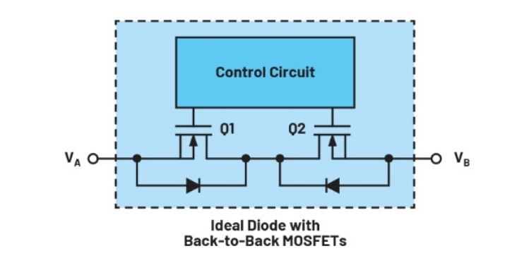
Thanks to advances in MOSFET technology, there are now low-RDS (ON) MOSFETs. If you add back-to-back MOSFETs to an ideal diode solution, although the voltage drop will be slightly increased, it will also bring many system control functions. Figure 2 shows this circuit concept.
Figure 2: An ideal diode with back-to-back MOSFETs
The original Q1 can control and block the reverse current from VB to VA. The addition of MOSFET Q2 can control and block the forward current from VA to VB. This solution enables complete system control by turning one or both MOSFETs on/off, or by limiting the flow of current in either direction.
Application examples and main specifications of ideal diode
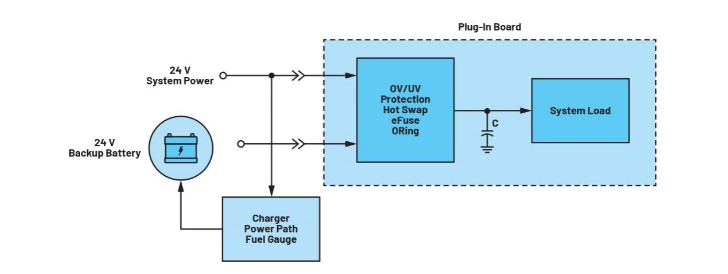
Ideal diodes have many applications. Take an industrial UPS backup power system (Figure 3) as an example. The system uses 24V main power supply. This power supply operates from 19.2VDC to 30VDC, with transient voltages up to 60V. Use the 24V battery as a backup power source. To ensure that backup power is fully available, the battery is charged to 24V during normal operation (when the battery is in standby mode). When the main power supply is interrupted, the battery provides backup power, discharging from 24V to 19.2V or less until the system is no longer operating, or until the main power supply is restored, whichever occurs earlier. An ideal diode circuit is required to provide the ORing function for switching between the system power supply and the backup battery. In addition to the ORing function, the system requires overvoltage, undervoltage, hot swap, and eFuse protections to protect against common system failures and enhance system robustness.
Figure 3: Industrial UPS backup power system
ORing and source selector
Figure 4 shows the power ORing concept. For simplicity, the diode symbol is used here instead of the ideal diode circuit. In this simple ORing configuration, the higher voltage power supply dominates and powers the load, and the other power supply is in standby. This solution works well if the two power supplies have different voltage values. When two voltages are close to each other, or when there are voltage fluctuations that cause voltage values to cross, the power supply may switch back and forth.
Figure 4: Input power ORing
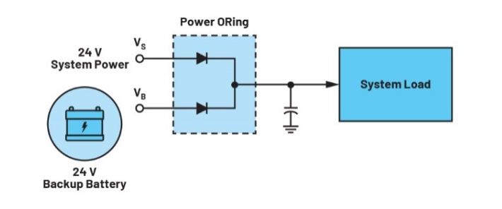
In this use case, the simple ORing functionality is insufficient for two reasons. First, the battery voltage is about the same as the system's nominal voltage of 24V. The two power supplies may switch back and forth, which we do not want to see. The influence of source impedance and load current further magnifies the problem. For example, when the VS powers a load, the load current creates a voltage drop at both ends of the VS source impedance, reducing its terminal voltage to a level slightly lower than the battery terminal voltage (currently unloaded).
The battery is then switched on and now carries the load current, which also creates a voltage drop at both ends of the battery impedance, causing the battery terminal voltage to drop. At the same time, in the absence of load, the main power supply terminal voltage rises, making VS try to take over. In this case, oscillations will continue between the two sources until the two voltages deviate from each other.
Second, 24V system power supplies have a voltage range of 19.2VDC(minimum) to 30VDC(maximum), and peak voltage transients can be as high as 60V. The backup battery voltage is charged to 24VDC, and when the main supply voltage drops below the battery voltage but is still within its operating range, it will be powered by the battery. This is also something we do not want to see, because the battery will discharge to a non-ideal standby voltage.
Whenever the system voltage is below 24V and above its minimum operating range, the system may attempt to charge and discharge the battery at the same time. A source selector is useful in this case. Figure 5 shows the source selector concept using an ideal diode with back-to-back MOSFETs. With back-to-back MOSFETs, the controller can completely cut off the current path in both directions, just like a mechanical switch is disconnected. Figure 6 is a symbolic representation of an ideal diode with back-to-back MOSFETs. This symbol in Figure 5 indicates that the source selector function can be implemented. In this configuration, VS is set to high priority. VB is off and only switched on when VS is below its operating voltage range.
Figure 5: Input source selector
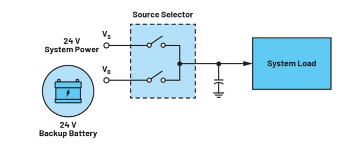
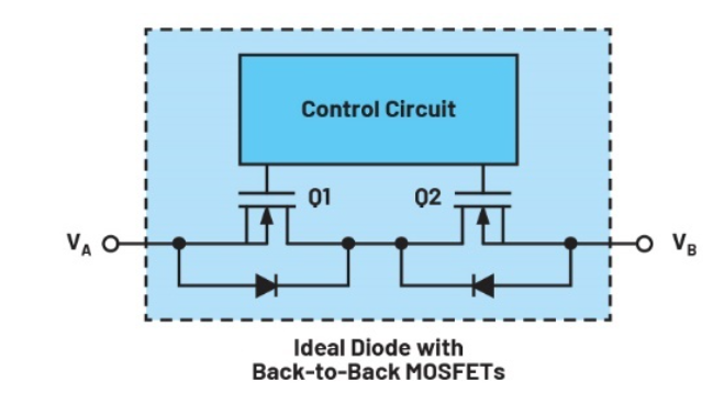
Figure 6: Symbolic representation of an ideal diode with back-to-back MOSFETs

Figure 7: Shows the power selector operation during battery standby and standby.

Other important system protection requirements
Although Figure 6 shows a mechanical switch that is on or off, note that the controller can also adjust the current with the appropriate current detection circuit. Important functions such as surge limitation (hot swap), overload/short circuit protection (eFuse), and undervoltage/overvoltage (UV/OV) can be achieved using existing MOSFETs of the same power.
Hot swap
As shown in Figure 3, when the board is plugged into the backplane (the board where the primary system power and backup batteries are located), the system board requires a hot-swappable function to limit the surge current when charging the input capacitor C. This hot swap function is achieved by detecting and controlling the current flowing through Q2 in Figure 2.
eFuse
This feature protects the system from overcurrent or short circuit conditions. Using the same Q2 in Figure 2, the current flowing through Q2 can be monitored, limited, and turned off. The accuracy of current limiting thresholds in eFuse applications is very important to optimize the system power budget.
UVIOV
The controller continuously monitors the power supply voltage. Undervoltage protection (UVLO) keeps Q2(Figure 2) safely off until the supply voltage rises above its lowest operating level (19.2V in this example). When the input transient voltage exceeds the set maximum level (in this example, select the voltage value > At 30V), the overvoltage protection (OV) function will turn off Q2.
Important ideal diode circuit specifications and their effects on system performance
We return to the ideal diode and examine some of its key specifications when used in the ORing or source selector function.
Reverse current response time
Referring to Figure 2, this is the time Q1 is turned off after the voltage VA and VB are reversed and VB is greater than VA. This reverse current response time tR must be small (100 ns) to prevent the reverse current from flowing back from VB to VA. In this system, the voltage may reverse when the main power supply VS(while driving the load) is turned off, transitioned to a lower voltage, or short-circuited. In this case, the tR prevents the reverse current from flowing back to VS from board capacitor C or from the backup battery, or minimizes the reverse current as much as possible.
Recovery after overpressure
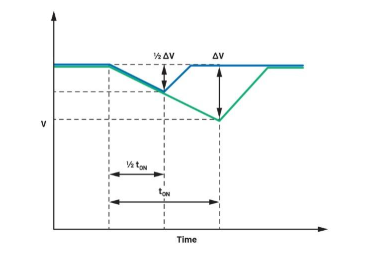
In a system without a backup battery (Figure 8), capacitor C provides backup power and is often referred to as a holding capacitor. In this configuration, a transient overvoltage condition on VS triggers a Q2(Figure 8) shutdown. The capacitor provides the necessary power to keep the system running while its voltage drops due to discharge. When VS returns to its normal operating range, Q2 is switched on again. Q2 reconduction time tON must be very short, so that the capacitor voltage drop is as low as possible. Figure 9 shows a comparative result where a half tON can reduce the voltage drop by half while maintaining the same capacitance.
Figure 8.:System with holding capacitance
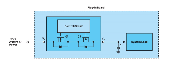
Figure 9: Relationship between pressure drop and tON
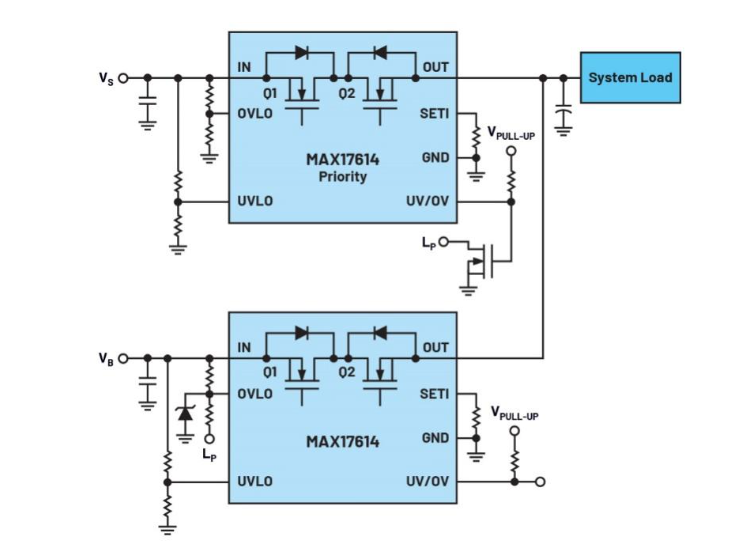
Different features such as source selector, hot swap, eFuse, UV/OV and critical specifications are investigated with the aim of preventing common system failures and enhancing system robustness. Using many single-function ics to implement all of these functions can be cumbersome. This solution is complex and requires many components. The MAX17614 is a new, highly integrated solution that enables high performance ideal diode functions and many other functions from a single C to provide complete protection for power systems. The device operates in a voltage range of 4.5V to 60V, offers 3A output, ideal diode/priority power selector functionality, and adjustable current limiting, hot swappable, eFuse, UV and OV protection. Figures 10 and Figures 11 show simplified schematics of the MAX17614 in the ORing application and priority power selector application, respectively.
Figure 10: Voltage 0Ring application for MAX17614
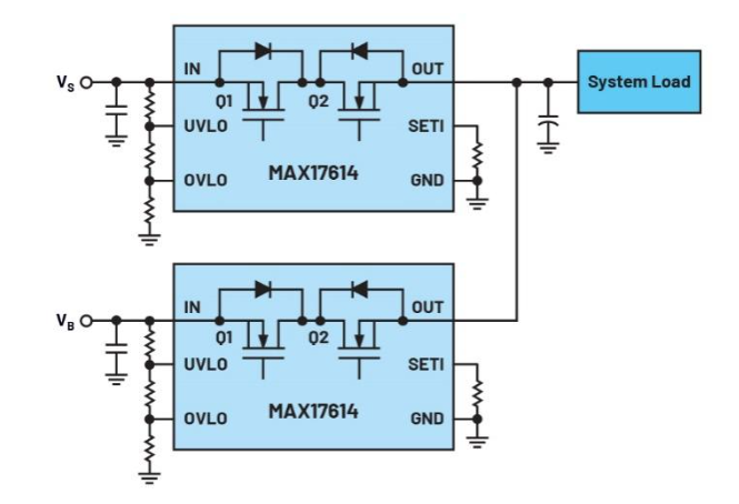
Figure 11: Priority power selector application for the MAX17614, where VS has priority
Conclusion
Back-to-back MOSFET solutions provide additional system control functions such as source selection, hot swap, eFuse, UV/OV, and more. Traditional solutions that use a combination of single-function ics to provide complete system protection are complex and cumbersome. We examine UPS backup power applications and briefly describe an ideal diode solution that also integrates other required functions into a single IC for overall system protection.
About US
Heisener Electronic is a famous international One Stop Purchasing Service Provider of Electronic Components. Based on the concept of Customer-orientation and Innovation, a good process control system, professional management team, advanced inventory management technology, we can provide one-stop electronic component supporting services that Heisener is the preferred partner for all the enterprises and research institutions.