Silicon Lab's ultra-low power digital isolators family are CMOS devices that offer significant data rate, propagation delay, power, size, reliability, and external BOM advantages over traditional isolation technologies. The operating parameters of these products remain stable over a wide temperature range and throughout the service life of the equipment for easy design and highly uniform performance.
Pin Descriptions

All device versions have Schmidt trigger input for high anti-jamming and require only VDD bypass capacitors. Data rates of up to 150mbps are supported, with propagation latency of less than 10ns for all devices. Enabling input provides a single point of control for enabling and disabling output drivers. Ordering options include selection of isolation ratings (1.0,2.5,3.75 and 5 kV) and optional fail-safe operating modes to control the default output state during power loss.
All products > All 1kv are UL, CSA, VDE and CQC safety certified, and the products support enhanced insulation in wide-body packaging and can withstand up to 5kvrms. Car grades can be used for some parts numbers. These products are built using car-specific processes at all steps in the manufacturing process to ensure the robustness and low defects required for automotive applications
The Si864x channel works like an optical coupler, except that it modulates an RF carrier instead of light. This simple architecture provides a robust isolated data path that requires no special consideration or initialization at startup. A simplified block diagram of a single Si864x channel is shown below
Simplified Channel Diagram 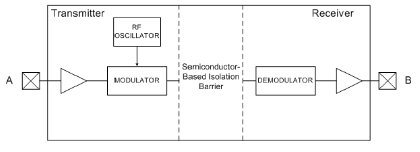
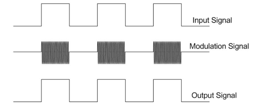
The channel consists of an RF transmitter and an RF receiver separated by a semiconductor-based isolation barrier. Referring to the transmitter, input A uses the carrier provided by the on/keys-modulated RF oscillator. The receiver contains a demodulator that decodes the input state according to its RF energy content and applies the result to output B via an output driver. This RF on/key control scheme is superior to the pulse coding scheme because it provides first-class anti-jamming, low power consumption, and improved anti-jamming to magnetic fields. See the chart below.
Modulation Scheme