In recent years, the automotive industry is rapidly entering a new era of intelligence and electrification. Sales and market penetration of new energy vehicles continue to rise. According to Bloomberg, global sales of new energy vehicles will reach 14.1 million units in 2023, of which the Chinese market will account for about 60%. Despite the focus on third-generation semiconductor materials such as SiC and GaN in the automotive transition to electrification, EV manufacturers remain conservative about costs. Cost-effective and stable silicon-based MOSFETs (metal-oxide-semiconductor field-effect transistors) continue to play a central role in in-vehicle electronics, electric drives and battery management systems. This was further highlighted by the massive shortage of MOSFETs last year.
However, to meet the growing automotive market, power MOSFETs require continuous technological innovation to meet numerous challenges such as higher switching frequencies, greater power density and lower power consumption. In the face of these changes and challenges, as a leader in the development and production of basic semiconductor devices, how does Nexperia, which wins with efficiency, secure its foundation and meet the development of the new era of automotive? What transformative steps have been taken to advance automotive MOSFET technology?
Packaging technology develops to accelerate the gear rotation
At present, the use of semiconductor devices in new energy vehicles has reached a record number, and the urgent need for small, high-performance and reliable devices runs through almost all electronics markets. In this trend, packaging technology is playing a crucial role.
In the early days of semiconductors, packaging mainly relied on Through-Hole Technology (THT), of which TO-3 is a representative packaging technology. With the development of technology, the size of electronic equipment is gradually reduced, and the integration of components is increasingly required. This has led to the emergence and widespread application of Surface Mount Technology (SMT). Compared to THT, SMT components are smaller and lighter and can be soldered directly to the surface of the board without the need to punch holes. This greatly improves production efficiency and reduces the size of components.
The development of surface mount technology (SMT) has played a great role in promoting the progress of MOSFET.
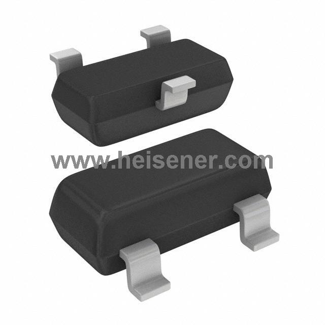
The first is SO-8 packaging technology, which became popular in the 1980s. It is usually rectangular, as its name suggests, and SO-8 has four pins on each side for a total of eight pins. SO-8 packages are typically made of plastic with a metal pin frame inside to connect the chip to the external circuitry. The SO-8 package provides a compact solution for MOSFETs while maintaining modest power handling capabilities.
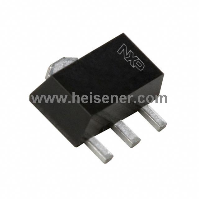
In the early 1990s, two surface mount packaging technologies, DPAK (TO-252) and D2PAK (TO-263), became popular in response TO the need for better heat dissipation in automotive electronics and industrial applications. They are both 3-pin designs and both feature metal housings, which are larger in size compared to DPAK and are often used for higher power applications. For a long time, automotive power MOSFETs have relied primarily on these two older and larger lead-bonded packages. However, with the industry's demand for small size, high power density and high current processing capacity, these two packaging technologies are gradually unable to meet the demand.
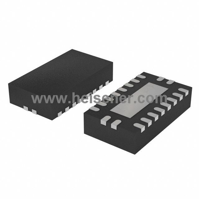
In 2004, Nexperia introduced a new package technology, the LFPAK copper clip package, which has a similar size to the SO-8 but offers significant efficiency and performance advantages over the DPAK and D2PAK.
So, how does this work? In the D²PAK and its variants, a cable connection is usually used between the chip and the package outlet, which limits the amount of current it can handle. Nexperia's LFPAK uses copper clip technology that provides a larger area of contact between the chip and the outlet, allowing it to handle larger currents and increase output power. And the copper clip also enhances the heat dissipation of the top and bottom of the chip.
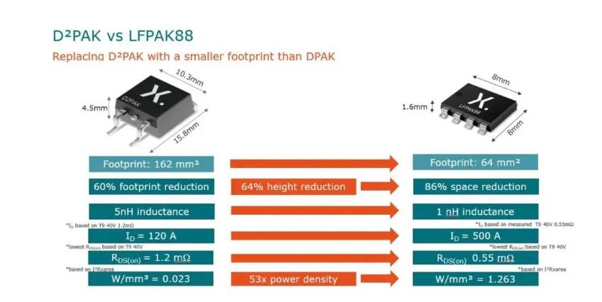
Especially with the introduction of LFPAK88, the excellent performance of LFPAK copper clip packaging technology has been fully verified. The LFPAK88 comes in a compact package size of 8mm x 8mm, providing space savings of up to 60% compared to the D²PAK (see Figure 1). What's even more remarkable is that despite its smaller size, the LFPAK88's performance is able to achieve up to 2x higher continuous current ratings, ultimate thermal performance and reliability.
The LFPAK88 is an ideal replacement for the D²PAK. Currently, Nexperia offers two versions of the AEC-Q101 for automotive and the industrial grade. LFPAK88 is not only widely used in automotive power steering, ABS braking, DC/DC conversion and other fields, but also suitable for battery isolation, battery powered tools and electric fuse motor control and other industrial fields.
Nexperia's BUK7S0R5-40H is a representative of the LFPAK8 copper clip package. This is an n-channel MOSFET that meets automotive certification standards and even exceeds the AEC-Q101 standard, with a wide temperature range of -55°C to +175°C, especially suitable for high temperature environments. Using the latest 40V Trench 9 low resistance overjunction technology, the product achieves RDSon as low as 0.55mΩ at the same size by reducing cell spacing and utilizing super construction.
Compared to the standard Trench MOS, it has enhanced SOA (safe operating zone) and avalanche capability, and strict limitations on V GS(th) (gate threshold voltage) make the parallel application of MOSFETs easier. It is used in a wide range of applications, including 12V automotive systems, 48V DC/DC conversion systems (12V secondary side), high power motors, lighting and solenoid valve control, reverse polarity protection, and other applications requiring ultra-high performance power switches.
Figure 1: Size comparison of LFPAK88 and D2PAK
In the last decade, with the rapid development of mobile devices and Internet of Things technology, the demand for small and high-performance MOSFET packages has increased, and small package technologies such as QFN (four-sided flat pin-free package) and DFN (double flat pin-free package) have emerged. In applications that require high current, good heat dissipation, and high reliability, LFPAK packaging may be a better choice. But in low-power applications, such as small signal products (ssMOS), because the power variation is not as large and the thermal stress is relatively small, the DFN in the small package can fully realize its size advantages.
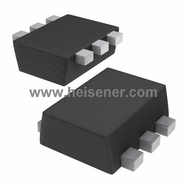
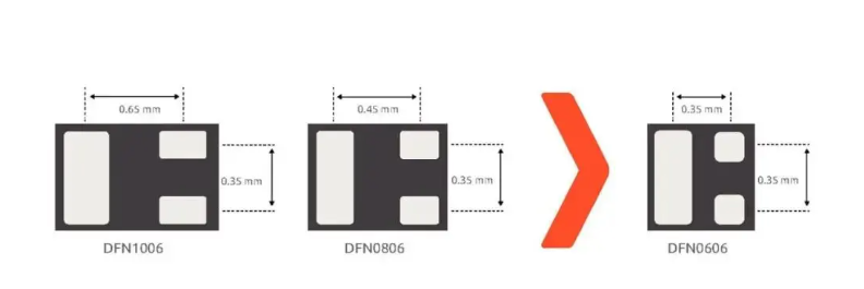
Nexperia's DFN0606 MOSFET package offers the tiniest DFN solution in the usual 0.35mm pitch size. This ultra-small package is ideal for situations where space footprint needs to be minimized, saving space while requiring little additional assembly work. This MOSFET package is ideal for applications in small mobile products such as wearables.
Figure 2: DFN0606 MOSFET subcompact package: Improved power efficiency, 0.35 mm pitch
MOSFET goes "focused"
In the past, standard power switches with a given factor of quality (FOM) could be used in virtually any situation. But with the advancement of technology and the diversification of applications, the demand for MOSFETs is more complex and diverse than ever before. There are more than 100 parameters on the regular MOSFET data sheet, such as Rds(on), Vth, Ciss, and Qg. But there are usually only a few parameters that matter in each project. And as applications change, so do key parameters.
Therefore, a single MOSFET parameter is difficult to meet the needs of all applications. Nexperia understands this, and "application-specific" is another major innovation in the MOSFET space, based on years of application-specific understanding and collaboration with customers. By focusing on optimizing the parameters that are most critical to a particular application scenario, even at the expense of other less relevant parameters, we ensure that our MOSFET products are perfectly matched to the needs of the specific field and bring out the best performance and benefits.
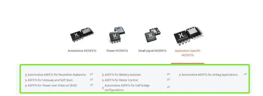
Nexperia has created a broader range of application-specific MOSFETs. As shown in Figure 3 below, it can be roughly divided into two categories: ASFET of vehicle level MOS and non-vehicle level ASFET, and their emphases are different. Among them, the hot-swappable ASFET LFPAK88 is currently mainly used in industrial and consumer electronics power supplies, and the ASFET of vehicle scale MOS is mainly used in half-bridge, repeat avalanche and airbag drive.
Figure 3: Overview of Nexperia application-specific MOSFETs
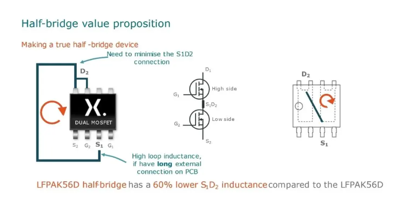
Half-bridge is a common term in the field of power electronics, specifically referring to a circuit topology. A half-bridge configuration is a standard building block in many automotive applications, in which two switching elements (typically two MOSFETs or IGBTs) are connected in series between the power source and the ground. When one switch is on, the other is off. By switching these two switches alternately, the voltage and current direction of the load can be controlled.
Nexperia's LFPAK56D half-bridge product is a representative of application-specific MOSFETs, and due to the removal of PCB wiring, it takes up 30% less PCB area than the dual LFPAK56D (Figure 4). Moreover, due to the copper clip connection between the MOSFETs, the parasitic inductance is reduced by 60% (Figure 5). The LFPAK56D half-bridge is AEC-Q101 automotive certified and provides the automotive industry with a range of plug-and-play solutions with superior current handling capabilities. It can be widely used in three-phase automotive powertrain applications (fuel pumps, oil pumps and water pumps), motor control, DC/DC and other automotive applications.
Figure 4: The LFPAK56D half-bridge takes up 30% less PCB area than the dual LFPAK56D
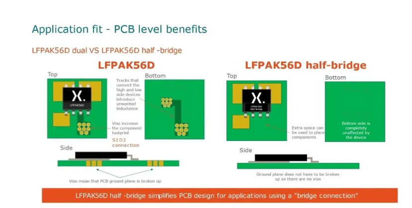
Figure 5: The parasitic inductance of the LFPAK56D half-bridge is reduced by 60%
The BUK7V4R2-40H product uses the LFPAK56D half-bridge package, which not only reduces the PCB layout complexity, but also shrinks the PCB by reducing the component size of the three-phase motor drive. The optimized package design improves system-level Rth (j-amb), supports higher efficiency with lower parasitic inductance, and is compatible with LFPAK56D dual package. By using the advanced AEC-Q101-class Trench 9 silicon technology, low power losses and high power density are achieved with superior avalanche performance. In addition, its unique gull-wing leads support high manufacturability and automatic optical inspection (AOI).
About US
Heisener Electronic is a famous international One Stop Purchasing Service Provider of Electronic Components. Based on the concept of Customer-orientation and Innovation, a good process control system, professional management team, advanced inventory management technology, we can provide one-stop electronic component supporting services that Heisener is the preferred partner for all the enterprises and research institutions.